

In this example we demonstrate how to model through MaxLLG a regular unloaded patch antenna and obtain its main quantities such as an input scattering parameter ( ) and radiation patterns [1]. Fig. 1a gives an illustration of the antenna that is constructed of a ground plate, dielectric substrate, a microstrip feedline, and a radiating patch. Here, we consider the radiating patch of the length
  =16 mm and the width of
  =12.45 mm, loaded on the dielectric layer of thickness
  =0.8 mm with the relative permittivity
  of 12. The and parameters define the operating antenna frequency through the following equation:
(1) 
which with the chosen parameters gives  =6.7 GHz. However, the result might deviate from the theory due to fringing fields.
The first step is to create a 3D model for the simulation using FreeCad, where a number of cells in each direction must be identified. Since the thickness is much less than the in-plane geometry, it is efficient to set different cell size along  -axis and
  – and
– and  -axis: dx=dy=0.25 mm, dz=0.1 mm. For the sake of parameter, the feedline should be long enough so that the input signal and the reflected waveform were distinct from each other. Thus, the 3D model components have the following number of cells in three directions (, , and , respectively): the feedline – 10x130x1, the patch – 50x64x1, the dielectric substance – 90x214x8, the ground plane – 90x214x1. Each of these elements should be saved as step-file and uploaded then into the 3D CAD Files section, where material parameters (namely, magnetisation, conductivity, and dielectric constant) are set in SI units. Having the matrix file created, the metascript file should be filled in. The source here is represented as the -polarised electric field pulse applied between the ground plane and the feedline as depicted on Fig.1b. The output port is located about 40 cells away from the source in -direction. For all orientations perfectly matched layer (PML) boundary conditions should be ticked with number of the layers set in appropriate lines.
  -axis PML should be directed inward the structure, by 15 cells for instance, to suppress interference, while – and -axis PML, contrarily, should be separated from it by few cells not to interfere the radiation.
The resulting time domain data for  component is given in Fig.1c. One should pay attention on the flatness right after the input signal – the pulse spread must be chosen so that numerical dispersion wouldn’t erode the gap between the input signal and the reflection (in this example the spread is 200 time steps, and the first 4000 points are taken as the input pulse). Then, a Fourier transform of frequency-domain reflection coefficient is taken, where the first two drops correspond to the first mode (
 =2.66 GHz) and the second one (
 =3.17 GHz). The field patterns are provided in Fig.1e-f, that were obtained through continuous excitation on and , respectively.
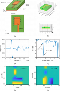
Fig. 1. a) Patch antenna schematic. b) Position of the source. c) Time domain data from MaxLLG simulation. d) Fourier transform of frequency-domain reflection coefficient. e-f) Field patterns, of the component for the first (e) and the second (f) modes.
[1] Orban D., The Basics Of Patch Antennas, Updated. 2009. URL: https://www.rfglobalnet.com/doc/the-basics-of-patch-antennas-updated-0001.